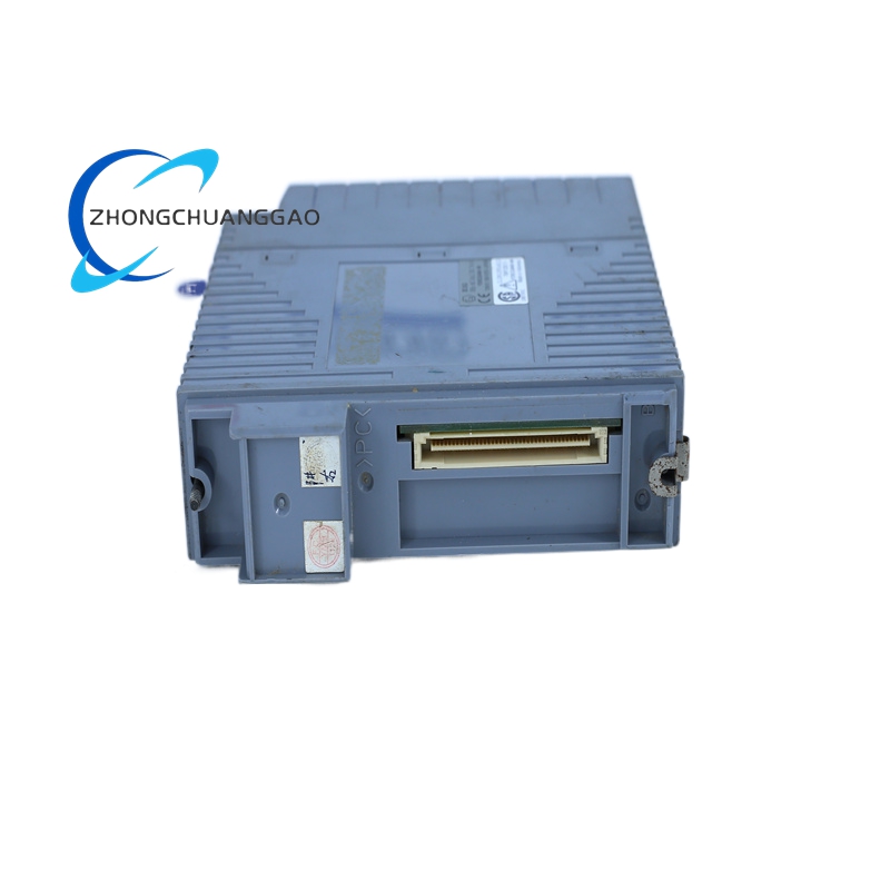
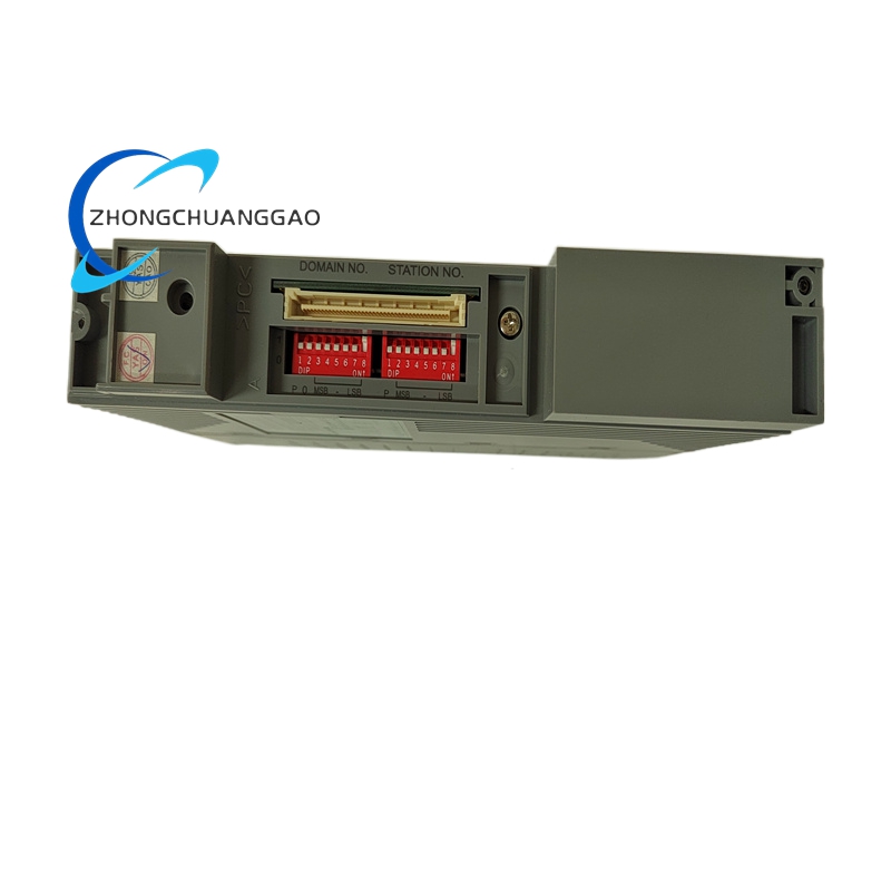
Product Introduction:
This semiconductor wafer inspection system is a highly advanced tool designed to detect defects on semiconductor wafers with extremely high sensitivity and accuracy. It uses a combination of optical, electron - beam, and other inspection techniques to scan the wafer surface and identify various types of defects, such as particles, scratches, pattern defects, and electrical defects. The inspection system plays a crucial role in ensuring the quality and yield of semiconductor manufacturing processes.
Technical Specifications:
- Inspection Techniques:
- Optical Inspection: Utilizes high - resolution optical microscopes and imaging systems to scan the wafer surface at different wavelengths of light.