Coating Material: Yttria-stabilized zirconia or silicon.
Wafer Size: 200 mm or 300 mm version according to chamber configuration.
Ring Width: 15–25 mm typical.
Operating Temperature: Up to 400°C.
Compatible Platforms: Listed sources associate it with Lam 2300 Flex, SPE, and Kiyo etch systems.
Function: Controls plasma sheath at wafer edge, reduces edge etch-rate variation, and limits particle generation.
Performance: Listed edge uniformity improvement from approximately ±15% uncorrected to ±3% with ring installed. Service life listed as 150–300 wafers depending on recipe.
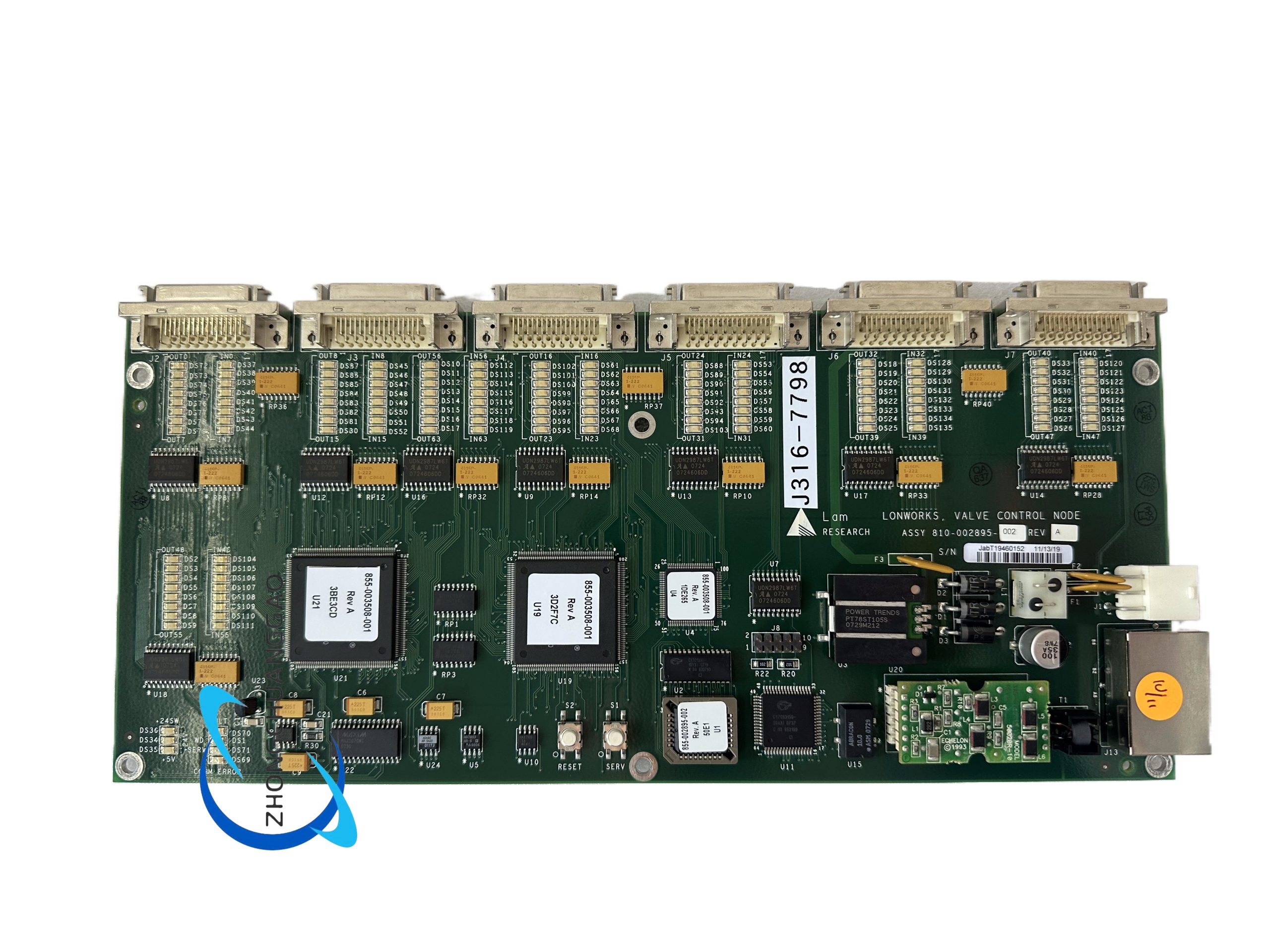
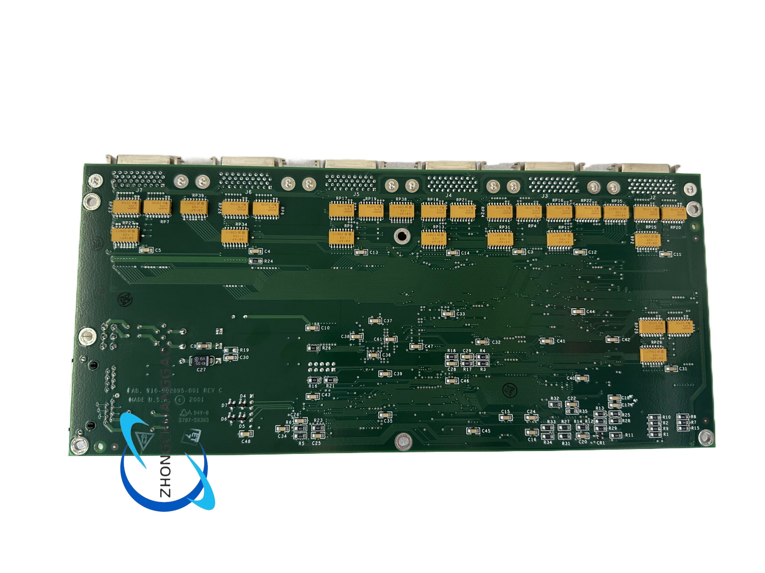
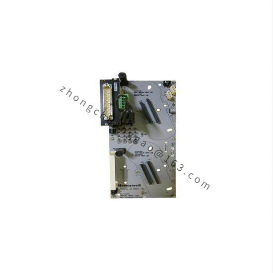
Option B – Valve Control / Node Control PCB
Product Type: LonWorks valve control node or I/O node control board.
Supply Voltage: 24 VDC ±10%.
Communication: LonWorks fieldbus or proprietary Lam node bus according to listed source.
Digital I/O: Models listed with 32 inputs and 32 outputs, 24 VDC, or valve-specific discrete I/O.
Analog Inputs: 0–10 VDC options listed for node-control variant.
Safety Interlocks: Dedicated interlock circuits on node-control listings.
Dimensions: 215 × 148 × 32 mm for valve-node listing; 220 × 160 × 25 mm for node-control listing.
Function: Controls pneumatic gas shutoff valves, mass flow components, vacuum isolation valves, indexing functions, and subsystem interlocks.
Working Principle
Focus ring option modifies electric-field distribution at wafer periphery to suppress edge effect. PCB option receives controller commands, drives valves or I/O devices, returns status, and executes interlock actions.
Installation Requirements
Focus ring: install concentrically on ESC or support pins, clean with IPA, verify wafer concentricity. PCB: power down tool, photograph DIP or jumper settings, seat in designated slot, verify firmware and node address.
Usage Precautions
Focus ring: inspect for cracks before each use, replace when edge uniformity exceeds specification. PCB: do not hot-swap, do not mix revisions, verify pinout before wiring.
Source Note
Because listed sources identify 810-002895-002 as either a focus ring or a control PCB, confirm the physical part, chamber platform, and Lam BOM before procurement or installation.