Digital guide

You are here:

Gasonics A95-053-02 C Electrode

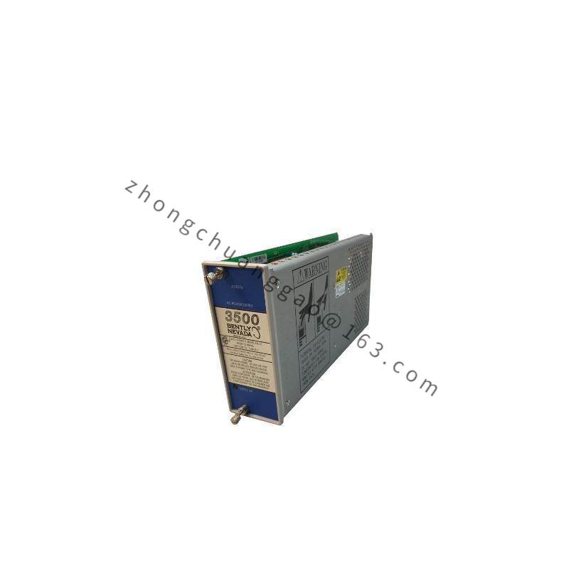
Product Description: This is a critical wear part, specifically an electrode or a component of the electrostatic chuck (ESC) assembly. The “C” revision typically indicates a material upgrade or a specific geometry change. It is the surface upon which the wafer sits and is often responsible for clamping the wafer electrostatically or mechanically and providing RF bias or cooling.

Technical Specifications:

  • Material: Single-crystal Silicon (for RF uniformity) or Aluminum Nitride (for thermal conductivity), coated with dielectric.

Detailed content

  • Diameter: Matches wafer size (200mm or 300mm)
  • Surface Finish: Ra < 0.1 microns for particle control
  • Cooling Channels: Micro-channels for helium backside gas cooling
  • Clamping Mechanism: Coulomb force (ESC) or edge clamp rings
  • Flatness: < 0.002 inches TIR (Total Indicated Reading)

Functional Features:

  • Wafer Clamping: Holds the wafer securely during plasma processing to prevent movement.
  • Heat Transfer: Efficiently transfers heat from the wafer to the cooling system (Helium backside gas).
  • Plasma Bias: If powered, it accelerates ions toward the wafer to control etch anisotropy or sputter rate.
  • Focus Ring: Often includes a replaceable focus ring to protect the main electrode edge from plasma.

Application Scenarios:

  • Ion Etching: Providing the bias power necessary for directional (anisotropic) etching.
  • Sputter Deposition: Acting as the cathode target or the substrate holder during PVD.
  • High-Temperature Processes: Withstanding temperatures up to 400°C during deposition or cure steps.
  • Low-k Dielectric Processing: Engineered to prevent charging damage to fragile low-k materials.

You may also like