Digital guide

You are here:

AMAT 0520-26789

Product Introduction
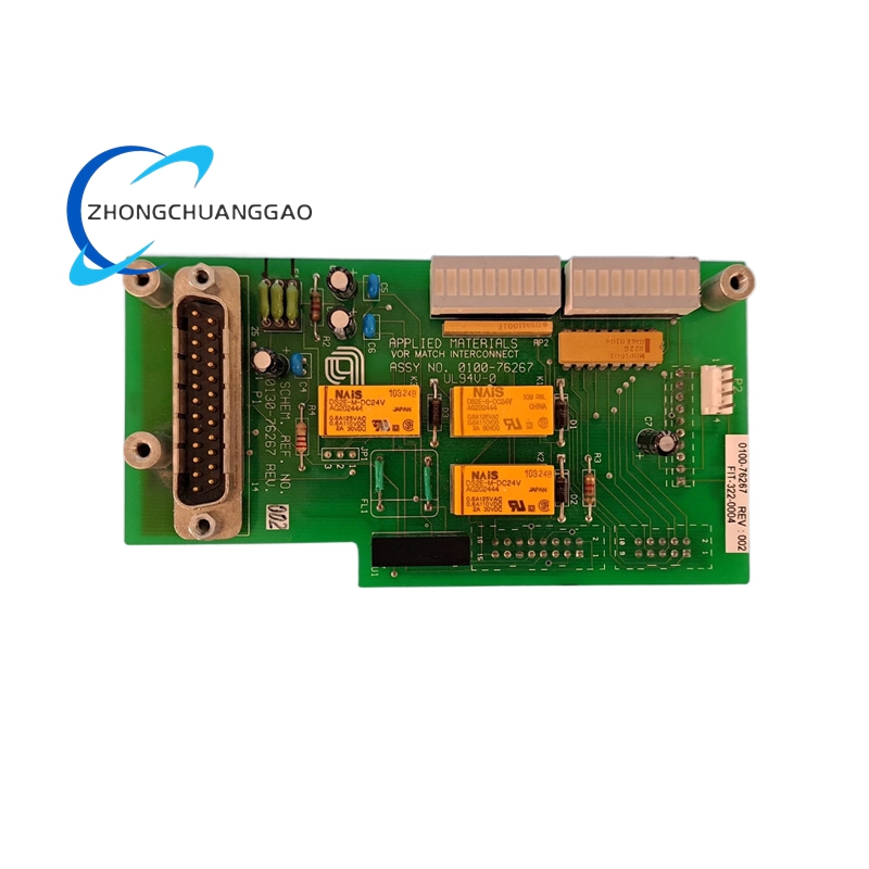
This is a critical component for semiconductor lithography equipment, which is used to transfer circuit patterns onto semiconductor wafers. Lithography is a fundamental process in semiconductor manufacturing, and the accuracy and quality of this transfer directly impact the performance and yield of the final semiconductor devices. This part plays a key role in enhancing the performance and reliability of the lithography process.

Technical Specifications

  • Resolution Capability: It enables the lithography equipment to achieve a high resolution, with the ability to print features as small as [X] nanometers (nm).

Detailed content

  • This high – resolution capability is essential for the fabrication of advanced semiconductor devices with increasingly smaller circuit patterns, such as those used in modern microprocessors and high – density memory chips.
  • Alignment Accuracy: The component provides extremely high alignment accuracy, with deviations of less than [X] nanometers in both the X and Y directions. Accurate alignment is crucial for ensuring that multiple layers of circuit patterns are precisely overlaid on top of each other during the lithography process, preventing misalignment – related defects.
  • Optical Transmission Efficiency: It has high optical transmission efficiency, allowing a large percentage of the light used in the lithography process to pass through without significant loss. This is important for achieving high – contrast images on the wafer, which improves the resolution and quality of the printed circuit patterns.
  • Thermal Stability: Given the high – power light sources used in lithography equipment, the component is designed to be thermally stable. It can withstand temperature variations without deformation or changes in its optical properties, ensuring consistent performance throughout the lithography process.

Functional Features

  • Enhanced Pattern Transfer: By providing high resolution and alignment accuracy, it enhances the pattern transfer process from the mask to the wafer. This results in more precise and accurate circuit patterns on the wafer, reducing the number of defects and improving the overall yield of the semiconductor manufacturing process.
  • Reduced Optical Aberrations: It helps in reducing optical aberrations such as spherical aberration, coma, and astigmatism in the lithography system. These aberrations can distort the image projected onto the wafer, leading to pattern distortions and reduced resolution. By minimizing these aberrations, the component ensures high – quality image formation.
  • Support for Advanced Lithography Techniques: It is compatible with advanced lithography techniques such as extreme ultraviolet (EUV) lithography and deep – ultraviolet (DUV) lithography. These techniques are used to fabricate the most advanced semiconductor devices, and the component’s high – performance characteristics enable it to support the demanding requirements of these technologies.
  • Long – Term Reliability: The component is designed for long – term reliability in the harsh environment of semiconductor lithography equipment. It is made from high – quality materials and undergoes rigorous testing to ensure that it can withstand the repeated exposure to high – intensity light and the mechanical stresses associated with the lithography process.

Application Scenarios

  • Leading – Edge Microprocessor Manufacturing: In the production of the latest generation of microprocessors with billions of transistors and nanometer – scale circuit patterns, high – resolution and accurate lithography is essential. This component is used in the lithography equipment to ensure that the complex circuit patterns are precisely transferred onto the wafers, enabling the fabrication of high – performance microprocessors.
  • High – Density Memory Chip Production: For high – density memory chips such as 3D NAND flash memory, where multiple layers of memory cells are stacked on top of each other, accurate lithography is crucial for the proper alignment of these layers. This part helps in achieving the necessary alignment accuracy, improving the storage capacity and reliability of the memory chips.

You may also like