AMAT 0310-15678
Product Introduction
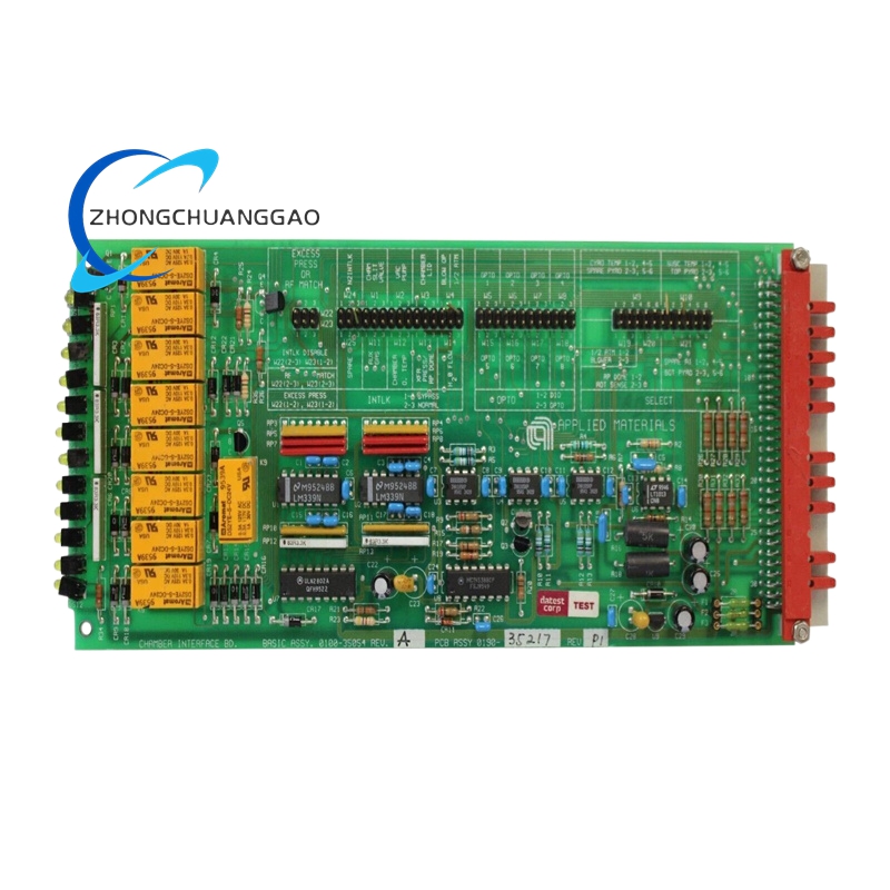
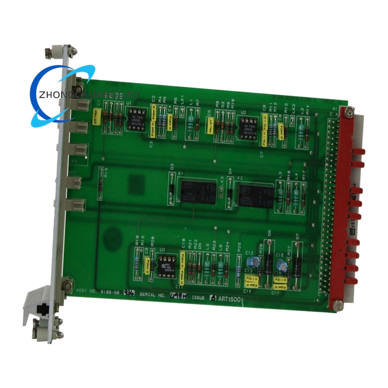
This is a high – precision component tailored for the semiconductor manufacturing industry, specifically engineered to enhance the performance of chemical mechanical polishing (CMP) equipment. CMP is a crucial process in semiconductor fabrication used to planarize the surface of wafers, ensuring uniform thickness and smoothness for subsequent processing steps. This part plays a vital role in optimizing the CMP process, contributing to the production of high – quality semiconductor devices.
Technical Specifications
- Pressure Control Accuracy: It can precisely control the pressure applied during the CMP process, with an accuracy of ±[X] psi (pounds per square inch).
Detailed content
- This level of precision is essential as different materials and layers on the wafer require specific pressure settings to achieve optimal polishing results without causing damage.
- Rotation Speed Range: The component allows for a wide range of rotation speeds, from [X] to [X] revolutions per minute (RPM). This flexibility enables it to adapt to various polishing requirements, as different materials and polishing slurries may perform best at different speeds.
- Material Compatibility: It is made from materials that are highly compatible with the chemicals used in CMP slurries. These materials are resistant to corrosion and wear, ensuring long – term reliability and consistent performance even in the harsh chemical environment of the CMP process. For example, it may incorporate special ceramics or high – performance polymers.
- Dimensional Tolerance: The part has extremely tight dimensional tolerances, with deviations of less than [X] micrometers in critical dimensions. This precision ensures proper fit and alignment within the CMP equipment, which is crucial for achieving uniform polishing across the entire wafer surface.
Functional Features
- Uniform Polishing: By accurately controlling pressure and rotation speed, it helps in achieving a highly uniform polish across the wafer. This is important for ensuring that all areas of the wafer have the same thickness and surface quality, which is critical for the performance of the semiconductor devices fabricated on it. For instance, in the production of microprocessors, uneven polishing can lead to variations in electrical performance between different transistors on the same chip.
- Slurry Distribution Optimization: It can optimize the distribution of the CMP slurry on the wafer surface. Proper slurry distribution ensures that the polishing agents are evenly applied, enhancing the polishing efficiency and reducing the amount of slurry required. This not only saves costs but also minimizes the environmental impact associated with slurry disposal.
- Reduced Defect Generation: The high – precision design and control capabilities of this component help in reducing the generation of defects during the CMP process. By avoiding excessive pressure or uneven polishing, it prevents issues such as scratches, pits, and dishing on the wafer surface, which could otherwise lead to device failures.
- Real – Time Monitoring and Adjustment: Some advanced versions of this component may be equipped with real – time monitoring sensors. These sensors can detect changes in process parameters such as pressure, speed, and slurry flow rate, and make automatic adjustments to maintain optimal polishing conditions. This ensures consistent performance throughout the CMP process, even in the presence of variations in the input materials or environmental conditions.
Application Scenarios
- Advanced Logic Chip Manufacturing: In the production of high – performance logic chips, such as those used in servers and supercomputers, the CMP process is critical for achieving the required level of planarization. This component helps in ensuring that the multiple layers of materials on the chip are polished to the correct thickness and with high uniformity, enabling the fabrication of complex and high – density circuits.
- Memory Device Production: For memory devices like dynamic random – access memory (DRAM) and NAND flash memory, uniform polishing is essential for reliable data storage and retrieval. This part is used in the CMP equipment during the production of these memory devices to achieve the necessary surface quality and thickness control, improving the overall performance and yield of the memory chips.


.jpg)


