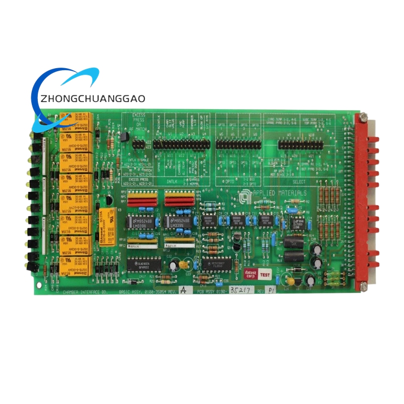
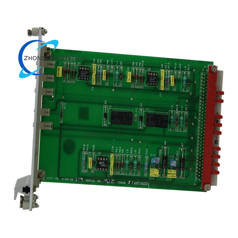
Product Introduction:
This component is an integral part of the vacuum chamber in semiconductor manufacturing equipment. The vacuum chamber is a crucial environment where various processes, such as physical vapor deposition (PVD) and chemical vapor deposition (CVD), take place under extremely low – pressure conditions. This component ensures the integrity and proper functioning of the vacuum chamber.
Technical Specifications:
Material: Made of high – strength stainless steel 316L, which has excellent vacuum compatibility and can withstand high – vacuum pressures down to 10^-9 Torr.
Shape and Size: It has a cylindrical shape with an outer diameter of 300 mm, an inner diameter of 280 mm, and a height of 500 mm. The wall thickness is 10 mm, providing sufficient strength to withstand the internal and external pressure differentials.
Surface Treatment: The inner surface is polished to a mirror finish with a surface roughness of less than Ra 0.05 μm. This reduces the adsorption of process gases and particles, maintaining a clean vacuum environment.
Functional Features:
Vacuum Sealing: It is equipped with high – quality O – ring seals made of a fluorocarbon elastomer material. These seals provide a reliable vacuum seal, preventing gas leakage into or out of the chamber.
Gas Inlet and Outlet Ports: There are multiple precisely machined ports for gas inlet and outlet. These ports are designed to ensure uniform gas flow within the chamber, which is essential for processes like CVD where a controlled gas environment is required.
Thermal Insulation: The outer surface of the component is coated with a thermal insulation layer to minimize heat transfer between the chamber and the external environment. This helps in maintaining a stable temperature inside the chamber during the manufacturing process.
Application Scenarios:
Physical Vapor Deposition (PVD) Systems: In PVD processes such as sputtering, it provides a clean and stable vacuum environment for the deposition of thin films on the wafer surface.
Chemical Vapor Deposition (CVD) Reactors: It is used to create the necessary vacuum conditions for the chemical reactions to occur, enabling the deposition of high – quality dielectric and conductive films on the semiconductor substrate.


.jpg)


