Digital guide

You are here:

AMAT 0040-98765

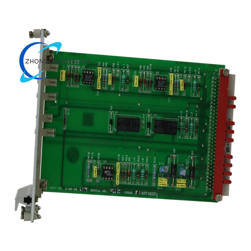
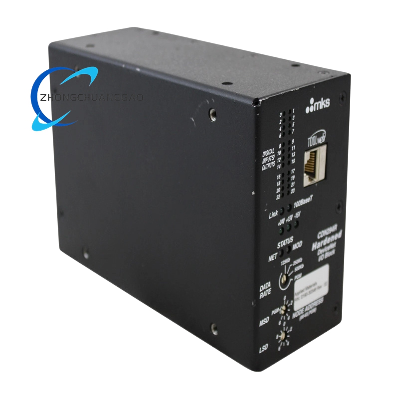
Product Introduction:
This semiconductor metrology tool is a highly precise instrument used for measuring various physical and electrical properties of semiconductor wafers and devices during the manufacturing process. It provides accurate and reliable data that is essential for process control, quality assurance, and yield improvement in semiconductor production.

Technical Specifications:

  • Measurement Techniques: Utilizes multiple measurement techniques, including optical metrology, electrical metrology, and scanning probe microscopy.

Detailed content

  • Optical metrology uses light – based methods such as ellipsometry and reflectometry to measure film thickness, refractive index, and surface roughness. Electrical metrology measures electrical properties such as resistance, capacitance, and conductivity. Scanning probe microscopy can provide high – resolution images of the wafer surface and measure features at the nanometer scale.
  • Measurement Range:
    • For film thickness measurement using optical metrology, it can measure thicknesses from [min_thickness] nanometers to [max_thickness] micrometers with an accuracy of ±[thickness_accuracy] nanometers.
    • In electrical metrology, it can measure resistances from [min_resistance] ohms to [max_resistance] mega – ohms with a resolution of [resistance_resolution] ohms.
    • Scanning probe microscopy can achieve a lateral resolution of [lateral_resolution] nanometers and a vertical resolution of [vertical_resolution] nanometers.
  • Sample Size: Can measure wafers with diameters ranging from [min_wafer_size] millimeters to [max_wafer_size] millimeters. It can also measure individual semiconductor devices on the wafer, depending on the measurement technique used.
  • Data Acquisition and Processing Speed: The tool has a high – speed data acquisition system that can collect measurement data at a rate of [data_rate] data points per second. The built – in data processing software can analyze the data in real – time, providing immediate feedback on the measurement results.

Functional Features:

  • Automated Measurement Routines: Offers automated measurement routines that can be programmed to perform a series of measurements on different locations of the wafer or device. This reduces the measurement time and improves the consistency of the measurement results.
  • Multi – Parameter Measurement Capability: Can measure multiple parameters simultaneously, such as film thickness and refractive index in optical metrology or resistance and capacitance in electrical metrology. This provides a more comprehensive understanding of the semiconductor sample and helps in identifying potential process issues.
  • User – Friendly Interface: Features a user – friendly graphical interface that allows operators to easily set up measurement parameters, view measurement results, and generate reports. The interface is intuitive and requires minimal training, making it accessible to a wide range of users.
  • Integration with Process Control Systems: Can be integrated with semiconductor manufacturing process control systems, allowing real – time feedback of measurement data to the process equipment. This enables automatic adjustment of process parameters based on the measurement results, improving process stability and product quality.

Application Scenarios:

  • Process Monitoring and Control: During semiconductor manufacturing processes such as deposition, etching, and lithography, the metrology tool is used to monitor key process parameters in real – time. For example, in a deposition process, it can measure the film thickness as it is being deposited, and if the thickness deviates from the target value, the process control system can adjust the deposition parameters to correct the deviation.
  • Quality Assurance and Yield Improvement: By measuring the physical and electrical properties of semiconductor wafers and devices, the metrology tool helps in identifying defective products early in the manufacturing process. This allows for timely corrective actions to be taken, reducing the number of defective products and improving the overall yield of the semiconductor production line.
  • Research and Development: In semiconductor research and development laboratories, the metrology tool is used to characterize new materials and processes. It provides detailed information about the properties of the samples, helping researchers to optimize the materials and processes for better performance and reliability.

You may also like