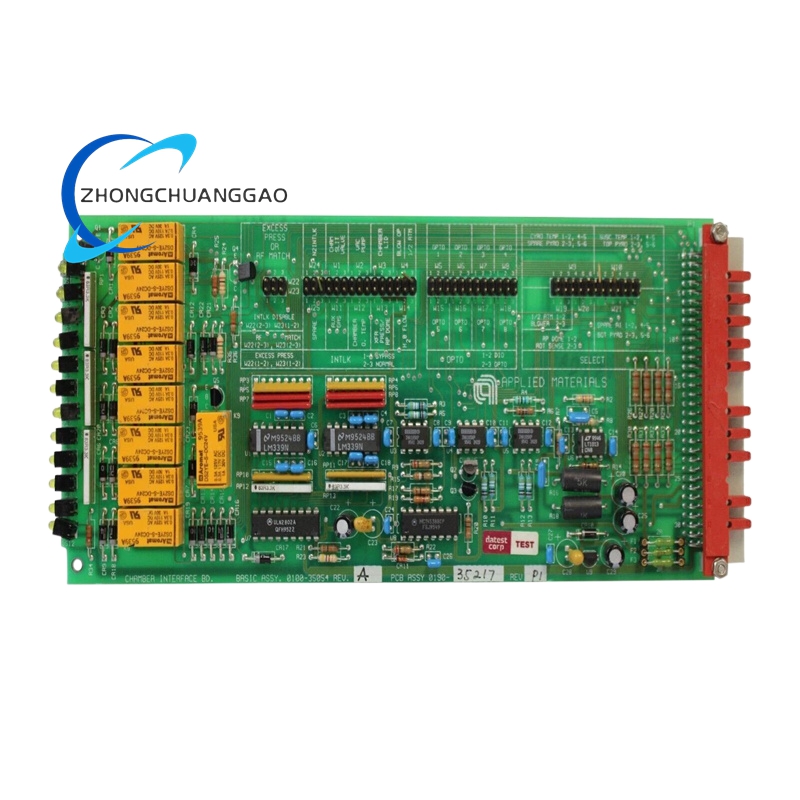
Product Name: Semiconductor Deposition System Component AMAT 0040 – 45149
Product Introduction: This component is a key part of semiconductor deposition systems, which are used to deposit thin films of various materials onto the wafer surface. Thin – film deposition is a fundamental step in semiconductor manufacturing, as it forms the basis for creating transistors, capacitors, and other electronic components. The AMAT 0040 – 45149 is designed to improve the quality, uniformity, and efficiency of the deposition process.
Technical Specifications:
Deposition Rate: Can achieve deposition rates ranging from a few angstroms per minute to several nanometers per minute, depending on the deposition method and material. This allows for precise control over the thickness of the deposited films.
Film Uniformity: Ensures high – uniformity deposition across the wafer surface, with less than 3% variation in film thickness. This is achieved through advanced gas distribution and plasma control technologies.
Material Compatibility: Supports the deposition of a wide range of materials, including metals (such as aluminum, copper, and gold), semiconductors (such as silicon and germanium), and insulators (such as silicon dioxide and silicon nitride).
Temperature Control: Has a precise temperature control system that can maintain the wafer temperature within a narrow range during the deposition process. This is important for ensuring the proper crystal structure and electrical properties of the deposited films.
Functional Features:
Plasma Enhanced Deposition: Utilizes plasma technology to enhance the deposition process. Plasma can activate the deposition gases, increasing the reaction rate and improving the quality of the deposited films. It also allows for low – temperature deposition, which is beneficial for heat – sensitive materials.
In – Situ Monitoring: Equipped with in – situ monitoring sensors that can measure the film thickness, composition, and other properties during the deposition process. This real – time feedback enables process optimization and quality control.
Automated Calibration: Has an automated calibration function that can adjust the deposition parameters based on the measured data. This ensures consistent and reliable deposition results over time.
Application Scenarios:
Solar Cell Manufacturing: Used in the production of thin – film solar cells, such as cadmium telluride (CdTe) and copper indium gallium selenide (CIGS) solar cells. The precise deposition capabilities of this component are crucial for creating high – efficiency solar cells with uniform film properties.
Optoelectronic Device Fabrication: Plays a role in the manufacturing of optoelectronic devices, such as light – emitting diodes (LEDs) and laser diodes. It helps in depositing the active layers and other functional films that are essential for the device’s optical and electrical performance.


.jpg)


