Digital guide

You are here:

AMAT 0040-03799

  • Technical Specifications:
    • Heating Material: Made from high – temperature – resistant materials such as kanthal alloy or silicon carbide. Kanthal alloy offers good electrical conductivity and can withstand high temperatures up to around 1400°C, while silicon carbide can operate at even higher temperatures, up to 1600°C or more, and has excellent thermal conductivity.
    • Power Rating: Has a specific power rating, usually measured in watts. The power rating is determined based on the size of the process chamber and the required heating rate. For example, a small – scale process chamber may use a heating element with a power rating of a few hundred watts, while larger chambers may require several kilowatts of power.

Detailed content

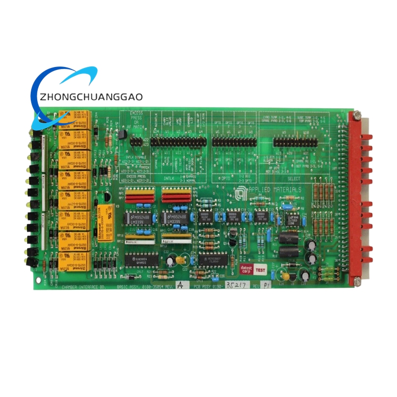
Temperature Control Accuracy: Can achieve high temperature control accuracy, often within ±1°C or better. This is crucial for semiconductor processes where precise temperature conditions are necessary for the proper formation of device structures and material properties.

  • Functional Features:
    • Uniform Heating: Designed to distribute heat evenly across the wafer surface. This is achieved through a carefully engineered heating element layout, such as a multi – zone heating design where different sections of the element can be independently controlled to compensate for any temperature variations within the chamber.
    • Fast Response Time: Has a relatively fast response time to changes in the power input, allowing for quick adjustments in temperature during the process. This is important for processes that require rapid heating or cooling cycles, such as in some types of annealing operations.
    • Long – term Stability: The heating element is built to withstand long – term use in the harsh semiconductor manufacturing environment, including exposure to high temperatures, reactive gases, and thermal cycling. It has a low degradation rate over time, ensuring consistent performance throughout its service life.
  • Application Scenarios: Installed in semiconductor process chambers for various thermal – based processes. In annealing processes, it is used to heat the wafer to specific temperatures to relieve stress, activate dopants, or repair crystal damage. During deposition processes like chemical vapor deposition (CVD), it provides the necessary heat for the chemical reactions to occur and form thin films on the wafer surface.

You may also like