AMAT 0020-99641
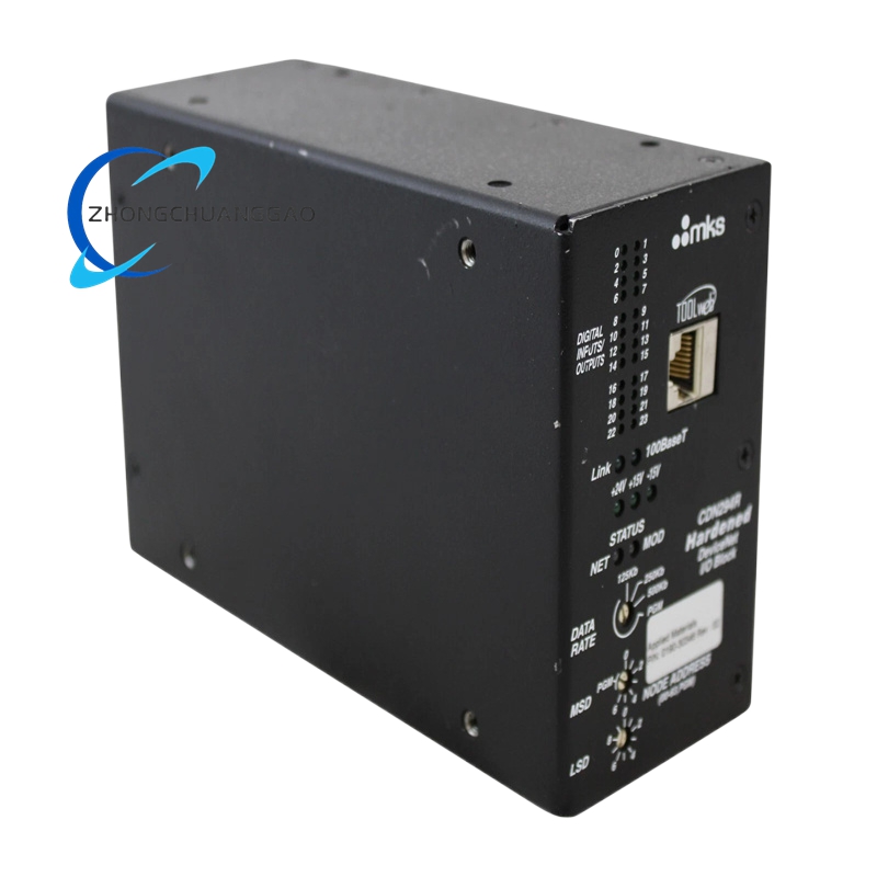
Product Introduction:
This is a critical component within the semiconductor manufacturing ecosystem, specifically engineered to enhance the performance and reliability of plasma – based processing equipment. Plasma processing is widely used in semiconductor fabrication for operations like etching, deposition, and surface cleaning. This part acts as a key enabler in controlling and optimizing the plasma environment, which is fundamental for achieving high – quality semiconductor device fabrication.
Technical Specifications:
- Electrical Conductivity: It boasts an extremely high electrical conductivity, measured in Siemens per meter (S/m), which allows for efficient transfer of electrical power to generate and sustain the plasma. The material used has a conductivity value that ensures minimal power loss during the plasma generation process, typically in the range of [X] x 10^6 S/m.
Detailed content
- Thermal Conductivity: Given the high – temperature environment in plasma processing, this component has excellent thermal conductivity. It can quickly dissipate the heat generated during plasma operations, preventing overheating of the surrounding equipment and ensuring stable process conditions. The thermal conductivity is in the order of [X] W/(m·K).
- Gas Permeability Control: It has precise control over gas permeability, which is crucial for regulating the flow of gases into the plasma chamber. The component can be designed with specific pore sizes or channels to allow the right amount of gases, such as argon, fluorocarbons, or oxygen, to enter the chamber at a controlled rate, influencing the plasma composition and properties.
- Mechanical Strength: Despite its need for specific electrical and thermal properties, it also has sufficient mechanical strength to withstand the mechanical stresses and vibrations present in the processing equipment. It can bear loads up to [X] Newtons without deformation or failure.
Functional Features:
- Plasma Generation and Stabilization: It plays a central role in generating a stable plasma by providing the necessary electrical path and controlling the gas flow. It helps in creating a uniform plasma distribution across the wafer surface, which is essential for consistent processing results. For example, in a plasma etching process, a stable and uniform plasma ensures that the etching rate is the same across the entire wafer, preventing over – etching or under – etching in different areas.
- Gas Flow Regulation: By precisely controlling the gas permeability, it can adjust the ratio of different gases in the plasma. This allows for fine – tuning of the plasma chemistry, which is critical for achieving specific etching or deposition characteristics. For instance, changing the ratio of fluorine – containing gases to oxygen can affect the selectivity of the etching process, enabling the removal of specific materials while leaving others intact.
- Heat Dissipation: The high thermal conductivity of the component helps in removing the heat generated during plasma operations. This prevents local hot spots in the plasma chamber, which could lead to non – uniform processing and damage to the wafer. It also protects other components in the equipment from heat – related failures, extending their service life.
- Corrosion Resistance: Since it is exposed to corrosive gases and plasma species during operation, the component has excellent corrosion resistance. It is coated with a special material or made from a corrosion – resistant alloy that can withstand the harsh chemical environment without degradation, ensuring long – term reliability.
Application Scenarios:
- Plasma Etching Equipment: In semiconductor etching processes, where precise removal of material from the wafer surface is required to create circuit patterns, this component is vital. It helps in generating a plasma with the right properties to etch specific materials, such as silicon dioxide, polysilicon, or metal layers, with high selectivity and uniformity. For example, in the production of microprocessors, it enables the creation of fine – line patterns with nanometer – scale precision.
- Plasma – Enhanced Chemical Vapor Deposition (PECVD) Equipment: In PECVD processes, where thin films are deposited on the wafer surface using plasma – activated chemical reactions, this component ensures the proper generation and control of the plasma. It allows for the deposition of high – quality films with good step coverage and uniform thickness, which are essential for the performance of semiconductor devices such as solar cells and thin – film transistors.


.jpg)
