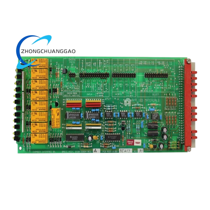
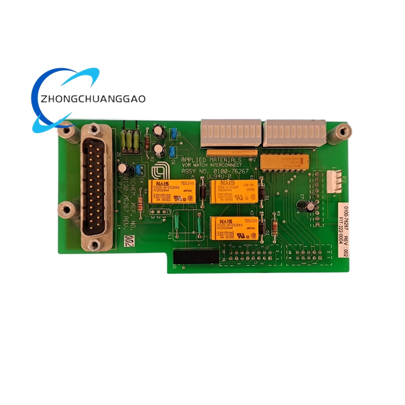
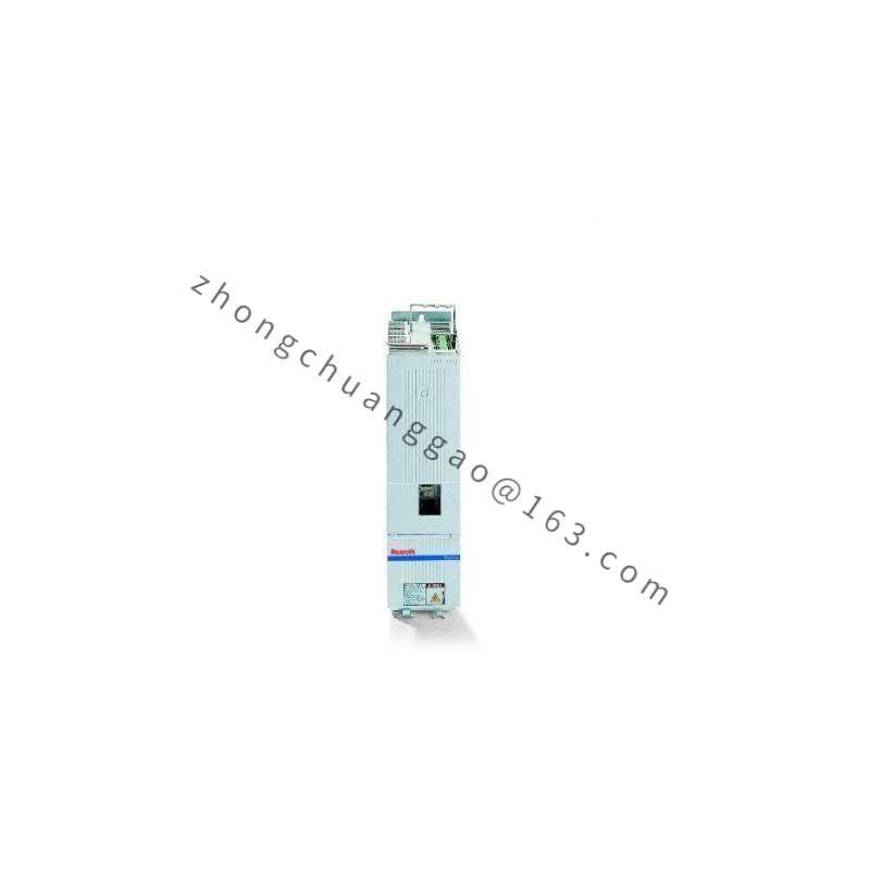
Product Name: AMAT 0020 – 43681 Plasma Etching Power Supply
Product Introduction: The AMAT 0020 – 43681 is a high – power plasma etching power supply used in semiconductor plasma etching equipment. Plasma etching is a key process for creating fine patterns on semiconductor wafers by selectively removing material using reactive plasmas. This power supply provides the necessary electrical energy to generate and sustain the plasma, enabling precise and efficient etching.
Technical Specifications:
Power Output: It can deliver a maximum power of 5 kW, with a wide adjustable power range from 100 W to 5 kW. This allows for flexibility in etching different materials and feature sizes on the wafer.
Frequency Range: Operates at a frequency range of 13.56 MHz, which is a commonly used frequency in plasma etching processes. This frequency provides a good balance between plasma generation efficiency and control over the etching process.
Voltage and Current Control: Offers precise voltage and current control, with a voltage regulation accuracy of ±0.5% and a current regulation accuracy of ±1%. This ensures stable plasma generation and consistent etching results.
Functional Features:
Fast Response Time: The power supply has a fast response time of less than 10 μs, allowing it to quickly adjust the power output in response to changes in the etching process conditions. This is crucial for maintaining uniform etching and preventing over – etching or under – etching.
High Efficiency: Designed with high – efficiency power conversion circuits, it can achieve an efficiency of over 90%. This reduces power consumption and heat generation, improving the overall energy efficiency of the plasma etching system.
Protection Features: It includes multiple protection features such as over – voltage protection, over – current protection, and arc detection and suppression. These features protect the power supply and the etching equipment from damage in case of abnormal operating conditions.
Application Scenarios:
Advanced Semiconductor Etching: Used in the etching of advanced semiconductor devices such as 3D NAND flash memory and high – k metal gate (HKMG) transistors. The precise power control and fast response time are essential for creating the complex and fine – pitched patterns required in these devices.
Research on New Etching Processes: In research laboratories, it enables scientists to explore new etching processes and materials by providing a stable and controllable power source for plasma generation.


.jpg)


