AMAT 0020-19643
Product Name: RF Match Network for CCP (Capacitively Coupled Plasma)
Product Introduction:
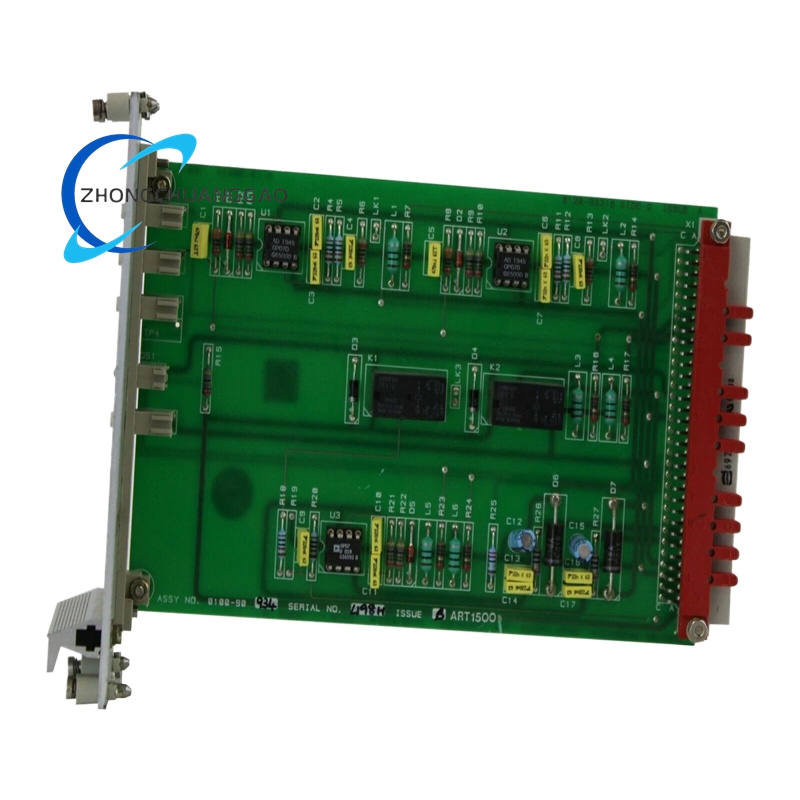
This is a specialized RF impedance matching unit designed for Capacitively Coupled Plasma (CCP) systems, often used in etch and CVD chambers. Unlike PVD match networks, CCP matches often deal with higher capacitance loads and different plasma ignition characteristics. This unit ensures efficient power transfer from the RF source (typically 13.56 MHz, 60 MHz, or dual-frequency) to the plasma electrodes (showerhead and pedestal). It is crucial for controlling ion energy distribution and plasma density independently in dual-frequency systems.
Detailed content
Technical Specifications:
- Configuration: L-Type or Pi-Type network (Inductor and Capacitors)
- Frequency: Single frequency (13.56 MHz) or Dual Frequency (e.g., 2 MHz / 60 MHz)
- Power Capacity: 1000W to 6000W depending on the chamber size.
- Tuning Elements: Motorized vacuum variable capacitors and fixed inductors.
- Cooling: Forced air or water cooling for the inductor and capacitor blocks.
- Control: Microprocessor-based with PID loops for fast tuning.
Functional Features:
- Dual-Frequency Control: In advanced units, it manages two separate RF inputs, allowing independent control of ion flux (low frequency) and ion energy (high frequency).
- Arc Suppression: Fast-acting crowbar circuits or fold-back circuits to protect the generator during arcing events common in CCP processes.
- Process Matching: Stores hundreds of recipes for different etch chemistries and pressures.
- Reflected Power Protection: Automatically shuts down RF if reflected power exceeds a safety threshold (e.g., 10%) to prevent generator damage.
- Analog/Digital Interface: Communicates with the tool’s system controller (SECS/GEM).
Application Scenarios:
- Dielectric Etch: Used in chambers for etching silicon dioxide, silicon nitride, and low-k dielectrics.
- Polysilicon Etch: Critical for gate etching in transistor fabrication.
- PECVD (Plasma Enhanced CVD): Used to deposit silicon nitride, oxide, and amorphous silicon layers.
- Sputter Etch/Pre-Clean: Used to remove native oxides before deposition.


.jpg)


.jpg)

