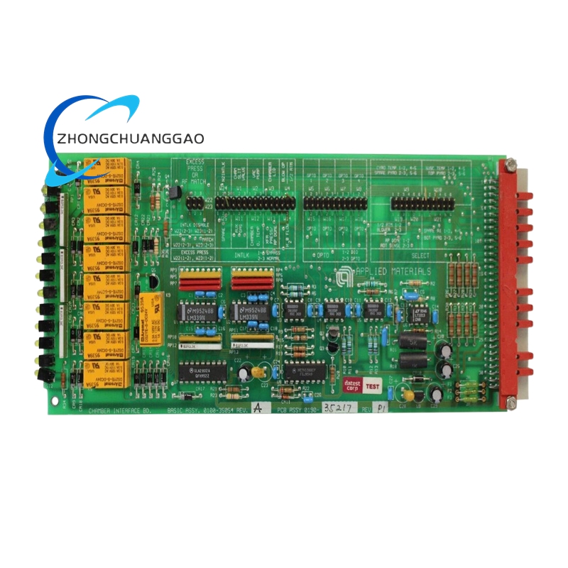
Product Introduction: The AMAT 0010 – 70322 is a high – precision component designed for use in advanced semiconductor etching chambers. It is a key element in the process of creating intricate patterns on semiconductor wafers, which is crucial for the production of modern integrated circuits. This component is engineered to operate reliably in the demanding environment of an etching chamber, where high – energy plasmas and reactive gases are used to remove material from the wafer surface.
Material Composition: Constructed from a specialized ceramic – metal composite material. This material offers excellent thermal stability, withstanding temperatures up to 500°C without significant deformation. It also has high chemical resistance, preventing corrosion from the reactive gases used in the etching process, such as chlorine – based and fluorine – based compounds.
Dimensions: The outer diameter of the component is precisely 300 mm, with a height of 150 mm. The internal cavity has a diameter of 250 mm and a depth of 120 mm, designed to accommodate specific wafer sizes and etching process requirements.
Electrical Conductivity: It has a low electrical resistivity of approximately 10^-6 Ω·m, which is essential for proper electrical connection and plasma generation within the etching chamber.
Functional Features:
Uniform Etching: The component’s surface is engineered to promote uniform plasma distribution across the wafer surface. This ensures that the etching process occurs evenly, resulting in consistent feature sizes and shapes on the semiconductor device.
Thermal Management: Its thermal properties help in dissipating heat generated during the etching process. This prevents overheating of the wafer and the component itself, which could lead to device damage or process inefficiencies.
Long – Term Stability: The material and design of the component allow it to maintain its performance over an extended period, even after repeated exposure to the harsh etching environment. This reduces the need for frequent replacement, lowering production costs.
Application Scenarios:
High – Volume Semiconductor Manufacturing: Used in large – scale production facilities where thousands of wafers are processed daily. Its reliability and performance contribute to high – yield production of advanced semiconductor devices, such as microprocessors and memory chips.
Research and Development Laboratories: In R&D settings, this component enables scientists and engineers to conduct precise etching experiments, exploring new materials and process parameters for future semiconductor technologies.


.jpg)

.jpg)
