Digital guide

You are here:

AMAT 0010-09195

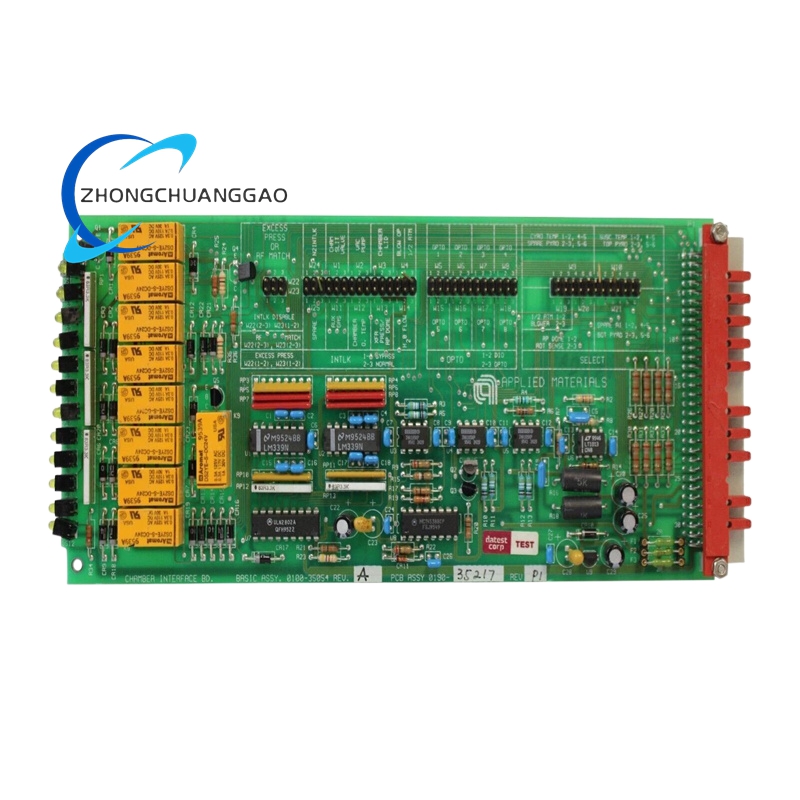
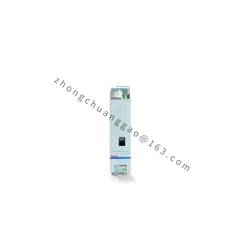
Product Introduction: This ion implanter is used to introduce dopant atoms into semiconductor materials to modify their electrical properties. It is a fundamental process in semiconductor manufacturing for creating the p – n junctions and other electrical structures in semiconductor devices.

Technical Specifications:

  • Can accelerate ions to energies ranging from a few keV to several MeV, depending on the doping requirements.

Detailed content

  • Has a high – precision beam control system to ensure accurate implantation of ions at the desired locations on the wafer.
  • Supports a wide range of dopant species, including boron, phosphorus, arsenic, and antimony.

Functional Features:

  • Precise Doping: The advanced beam control system allows for the precise control of ion implantation depth and dose, enabling the creation of well – defined electrical structures in semiconductor devices.
  • High – Energy Capability: The ability to accelerate ions to high energies makes it possible to implant dopants deep into the semiconductor material, which is necessary for some advanced device structures.
  • Dopant Versatility: The support for multiple dopant species makes the implanter suitable for a wide range of semiconductor materials and applications, from silicon – based devices to compound semiconductors.

Application Scenarios:

  • Used in the production of bipolar transistors and MOSFETs to create the p – n junctions and channel regions.
  • Employed in the fabrication of solar cells to dope the silicon material to improve its electrical conversion efficiency.
  • Integral part of integrated circuit manufacturing for creating the various electrical components on the chip.

You may also like